
Lithography Report
: Analysis on the Market, Trends, and TechnologiesThe lithography sector is at a decisive inflection: demand for advanced nodes and packaging is driving market expansion while company-level patent activity signals concentrated technological progress. The internal lithography trend report records 936 companies and total funding of $8.17B in the topic, with news coverage up 10.72% in five years, underscoring industry attention and capital flow. External market estimates vary by scope but cluster around a strong expansion: the global lithography equipment market was reported at USD 42.8B in 2024 and projected to grow to ~USD 93.1B by 2034 at an 8.4% CAGR Lithography Equipment Market Size – By Technology, Equipment, Application, End Use Industry Analysis, Share, Growth Forecast, 2025 – 2034. This report synthesizes core applications, emergent technology vectors, representative companies, and strategic implications for investors and manufacturing leaders.
Our latest update of this report was 266 days ago. If you found a mistake or missing information, tell us!
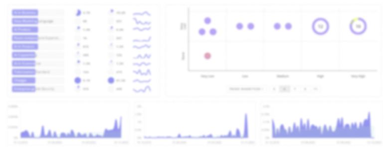
Topic Dominance Index of Lithography
The Topic Dominance Index evaluates Lithography's significance by analyzing data on the distribution of news articles that mention Lithography, the timeline of newly founded companies working in this sector, and global search trends
Key Activities and Applications
- Semiconductor patterning (front-end): high-resolution wafer patterning for logic and memory nodes remains the dominant revenue driver; EUV and DUV tools target sub-10 nm and multi-patterning requirements Lithography Equipment Market Opportunity, Growth Drivers, Industry Trend Analysis, and Forecast 2025-2034.
- Advanced packaging and 3D integration: fan-out wafer-level packaging, 3D IC stacking and heterogeneous integration increase demand for fine-pitch lithography in back-end processes Lithography Equipment Market Size – By Technology, Equipment, Application, End Use Industry Analysis, Share, Growth Forecast, 2025 – 2034.
- Nanophotonics/micro-optics production: periodic nanostructures for photonics and sensors require large-area, repeatable patterning techniques such as interference lithography and displacement Talbot approaches EULITHA PHABLE photolithography systems.
- Maskless/direct-write prototyping and low-volume manufacturing: maskless systems reduce lead time and cost for low-volume or customized runs, enabling rapid R&D and specialized device production Heidelberg Instruments maskless systems.
- Printing & packaging consumables: inks, coatings, and fountain/cleaning chemistries remain material submarkets with projected steady growth (e.g., lithographic printing chemicals market at USD 16.3B in 2023) Lithographic Printing Chemicals Market – By Product, By Application & Forecast, 2024 – 2032.
Emergent Trends and Core Insights
- Market bifurcation: a high-capital, high-precision branch focused on EUV/advanced-node semiconductor lithography and a broad, steady branch serving printing/packaging and specialty nano-applications; both present distinct investment logics Lithography Equipment Market Opportunity, Growth Drivers, Industry Trend Analysis, and Forecast 2025-2034.
- Computational augmentation: physics-informed ML and accelerated inverse lithography simulation reduce cycle time for mask/optical proximity correction and enable tighter process control, lowering R&D and ramp risk Inverse lithography technology based on a physics-guided reinforcement learning framework.
- Maskless and large-area periodic patterning scale-up: maskless digital approaches and interference-based systems (e.g., Zone-Plate-Array, Displacement Talbot) provide cost-effective routes for nanostructures and photonics over large substrates, addressing the scale/throughput trade-off for many non-leading-node markets LumArray ZPAL description and EULITHA DTL capabilities.
- Directed Self-Assembly (DSA) and nanoimprint: hybrid flows combining lithography with self-assembly or imprinting offer paths to sub-diffraction patterning at lower equipment cost per unit area Review of Directed Self-Assembly Material, Processing, and Application.
- Regional capacity build and geopolitical sensitivity: Asia Pacific and North America are focal growth markets due to foundry expansion and reshoring incentives; this heightens supplier concentration risk for extreme tools and materials Lithography Equipment Market Opportunity, Growth Drivers, Industry Trend Analysis, and Forecast 2025-2034.
Technologies and Methodologies
- Extreme Ultraviolet (EUV) and High-NA EUV: primary route for leading-edge logic nodes; capital intensity and resist/material challenges persist Market projections and EUV share discussion.
- Deep Ultraviolet (DUV) family (ArF, ArF immersion, KrF, i-line): workhorse for mid-to-back-end processes and many packaging flows; ArF remains large and growing for advanced packaging applications Market segmentation, ArF valuation 2024.
- Electron-beam and direct-write systems: niche high-resolution, low-volume use—important for masks, research, and specialized components xlith direct-write EBL service.
- Nanoimprint and SCIL (substrate conformal imprint lithography): high-throughput nanoscale patterning for optics and photonics with favorable cost-per-area characteristics SCIL Nanoimprint Solutions description.
- Laser direct imaging, thermal scanning probe (t-SPL), and zone-plate/interference techniques: enabling maskless, flexible patterning and 3D microstructure fabrication used in micro-optics, biomedical devices and prototyping Heidelberg Instruments and LumArray capabilities LumArray.
Lithography Funding
A total of 147 Lithography companies have received funding.
Overall, Lithography companies have raised $7.3B.
Companies within the Lithography domain have secured capital from 464 funding rounds.
The chart shows the funding trendline of Lithography companies over the last 5 years
Lithography Companies
- Lace Lithography: Small Norwegian team pursuing atom-based patterning to reach single-digit nanometer features with a reported energy-per-pattern advantage (claimed orders-of-magnitude efficiency). Their approach targets logic-scale disruption; technical validation and foundry adoption remain the critical next milestones Lace Lithography company entry.
- Heidelberg Instruments: Established provider of direct-write maskless laser lithography and thermal scanning probe tools for micro- and nanopatterning across photonics, MEMS and research markets; 1,500+ installed systems and process labs support customer ramp and process transfer Heidelberg Instruments company profile.
- LumArray, Inc.: MIT-derived maskless Zone-Plate-Array Lithography developer offering rapid-turnaround maskless patterning suited to low-volume, high-value photonics and MEMS production; attractive for customers needing fast iterations without mask costs LumArray company page.
- SCIL Nanoimprint Solutions: Commercial SCIL provider focused on wafer-scale nanoimprint for optics/photonic devices, delivering <10 nm features on large areas and aiming at high-volume optics manufacturing with tooling and consumables SCIL Nanoimprint Solutions profile.
Explore comprehensive profiles of 1.0K companies shaping the future of Lithography with TrendFeedr's Companies feature.
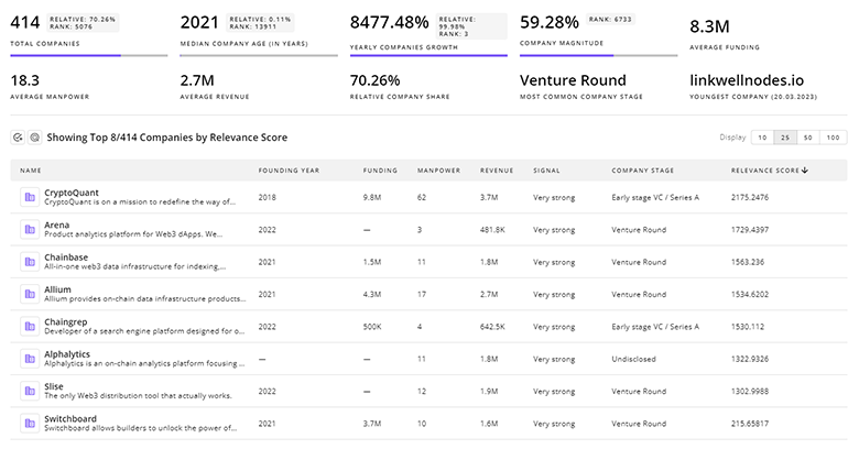
1.0K Lithography Companies
Discover Lithography Companies, their Funding, Manpower, Revenues, Stages, and much more
Lithography Investors
TrendFeedr’s Investors tool allows you to explore detailed investment activities and trends based on 481 Lithography investors. This tool provides an in-depth analysis of funding rounds and market dynamics to make informed investment decisions.
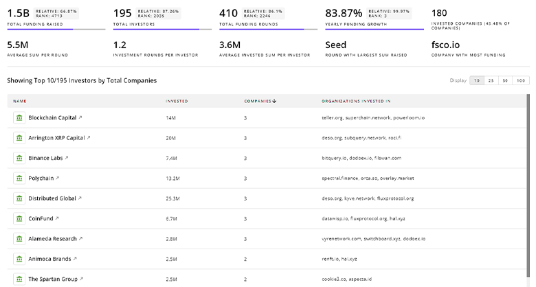
481 Lithography Investors
Discover Lithography Investors, Funding Rounds, Invested Amounts, and Funding Growth
Lithography News
Stay updated with TrendFeedr’s News feature, which offers you access to 5.6K Lithography articles. This tool provides you with a comprehensive understanding of the historical and current trends shaping the market.
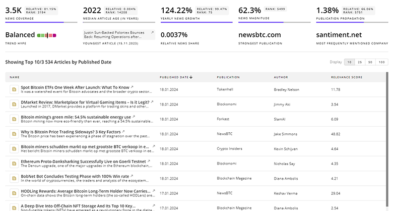
5.6K Lithography News Articles
Discover Latest Lithography Articles, News Magnitude, Publication Propagation, Yearly Growth, and Strongest Publications
Executive Summary
Lithography is a two-speed market: multi-billion-dollar capital investment for leading-edge node tools coexists with a broad addressable market of mid-range photolithography, maskless systems and consumables. Strategic winners will be firms that (1) align technology to a clear manufacturing window—EUV for leading nodes, DUV/Imprint/Maskless for packaging and photonics—(2) integrate computational controls to compress development cycles and improve yield, and (3) secure resilient supply chains for critical optics and materials. For investors and OEMs, the most attractive opportunities lie in platform plays that combine hardware, software and materials across high-growth niches (advanced packaging, photonics, nanoimprint) rather than undifferentiated component suppliers.
We’re keen to partner with subject matter experts to enrich our coverage. Think you can help? Let us know.


